“模拟域”部分将焦点放在IC、子系统和系统设计者面对的不断增长的电路设计挑战:接口ESD保护。沿着工业现有技术的轨迹,接口保护难度按两个趋势日益增加。首先,增加了处理速度和功能密度的需求,推动IC制造者进一步缩减MOS装置的最小尺寸。对给定的门绝缘体,设备原理上需要维持绝缘体厚度与横向尺寸成比例(参考文献1)。然而,较薄的绝缘体更容易受ESD的影响。
其次,端口速度持续增加,特别是便携式多媒体设备的兴起。例如,1996年发布的USB 1.0提供12Mbps的接口。四年后,USB 2.0达到480 Mbps。今年Intel开发者论坛出现,但仍未发布的USB 3.0,用平行光纤电缆替代铜连接器达到4.8Gbps的连接速度。IEEE 802.3(以太网)和IEEE 1394(火线)或多或少显示了趋势。
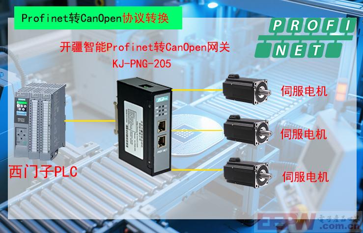
传统上,包括ESD分流结构,带标准互连焊盘单元的IC保护内部电路,避免ESD冲击设备引脚。如果其结构连接严格的抗ESD处理程序,对制造商而言,片上ESD保护板装配的IC安全是必要
这些结构不足的原因有两部分:它们太小到不能吸收接口常出现的瞬态大能量,远离接口入口点放置,防止邻近轨迹的耦合。一旦I/O线的片上ESD单元开始工作,瞬态电流沿走线增加,引起走线感应,产生相应瞬态电压,Ldi/dt。邻近I/O走线的互感导体满足超过其自身片上ESD单元容量的瞬态现象。这些邻近轨迹包括时钟、数据或其他非端口信号(参考文献2)。
装配TVS(瞬态电压干扰抑制器)到与入口点尽可能近,通过瞬态电流进入产品前分流ESD到地,来减少问题。这样做,用最小的附加费用,充分地增加了产品的鲁棒性。“如果手指接近节点,保护它”是一个好准则。尽管键帽是绝缘的,这个准则也应用到键区开关线。
高速接口需要带特殊低旁路电容的TVS。检查销售商的产品线,特别是高速接口设备。如果不能找到设备的特定接口,与销售商明确提供的标准接口比较信号频率和源线特性。考虑TVS制造商的要求,确保理解特定设备的ESD源模型。例如,JEDEC HBM(人体模型)通过1.5kΩ resistor,使用100pF电容放电。测试模型的可重复性结果历史上就是关注区域(参考文献3)。IEC-61000-4-2标准的测试方法提升了可重复性,其源模型——150Ω后的150pF——使设计要求更苛刻。
英文原文:
Protecting interfaces from ESD
Though on-chip-ESD structures serve as excellent secondary protection, they are usually insufficient to protect an interface over years of exposure in uncontrolled environments.
By Joshua Israelsohn, Contributing Technical Editor -- EDN, 12/3/2007
This installment of “Analog Domain” focuses on one of the growing circuit-implementation challenges that confronts IC, subsystem, and system designers alike: interface ESD protection. Two trends make interface protection increasingly difficult as we move along our industry’s current technology trajectory. First, increasing demands for processing speed and functional density have pushed IC fabricators to shrink further the minimum dimensions of MOS devices. For a given gate dielectric, device physics require maintaining the dielectric thickness in proportion to lateral dimensions (Reference 1). Thinner dielectrics, however, are more susceptible to ESD overstress.
Second, port speeds continue to increase, particularly with the growing success of portable-media devices. As one example, the 1996 USB 1.0 release provided for 12-Mbps interfaces. Four years later, a USB 2.0 feed could reach 480 Mbps. The yet-unreleased USB 3.0, shown at this year’s Intel Developer Forum, trades copper interconnect for parallel fiber-optic cable to attain a 4.8-Gbps connection. IEEE 802.3 (Ethernet) and IEEE 1394 (Firewire) show the trend to a greater or lesser degree.
Traditionally, ICs include ESD-shunting structures within their standard interconnect-pad cells, which protect the internal circuitry from ESD strikes to the device’s pins. The on-chip-ESD protection may be all that’s necessary to see an IC safely from its manufacturer to a board assembler if both organizations adhere to strict anti-ESD-handling procedures. Though on-chip-ESD structures serve as excellent secondary protection, however, they are usually insufficient to protect an interface over years of exposure in uncontrolled environments.
The reasons these structures are insufficient are twofold: They are too small to absorb large energy transients that interfaces commonly experience in the field, and they reside too far away from the interface-entry point to prevent coupling to adjacent traces. Once an I/O line’s on-chip-ESD cell begins to conduct, a current transient develops along its trace, exciting the trace’s inductance, causing a corresponding voltage transient, Ldi/dt. Adjacent conductors with mutual inductance to the I/O trace see coupled transients that can exceed the capabilities on their own on-chip-ESD cells. These adjacent traces can include clock, data, or other nonported signals (Reference 2).
Mounting TVSs (transient-voltage suppressors) as close to the entry point as possible alleviates this problem by shunting the ESD event to ground before transient currents develop inside your product. Doing so can add substantially to your product’s robustness with minimal additional cost. “If a finger can get close to a node, protect it,” is a good rule of … errrrr … thumb. This rule applies to keypad switch lines, too, despite their insulating keycaps.
High-speed interfaces require TVSs with particularly low shunt capacitances. Check your vendor’s product line for devices built for specific high-speed interfaces. If you don’t find devices specifically for your interface, compare your signalin
References
Sicard, Etienne and Syed Mahfuzul Aziz, “Application note on 45-nm technology,” Institut National des Sciences Appliquées de Toulouse, June 27, 2007.
“Disadvantage of on-chip transient protection,” Application Note SI97-04, Semtech, September 2000.
Verhaege, Koen, et al, “Recommendations to further improvements of HBM ESD component level test specifications,” Proceedings of the Electrical Overstress/Electrostatic Discharge Symposium, September 1996.
*博客内容为网友个人发布,仅代表博主个人观点,如有侵权请联系工作人员删除。